(China (Mainland))

Product Summary
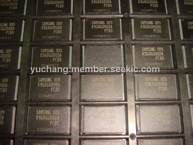
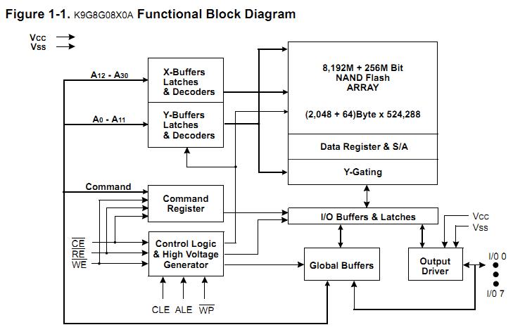
The K9G8G08U0A-PCBO is an 8,448Mbit(8,858,370,048 bit) memory organized as 524,288 rows(pages) by 2,112x8 columns. The memory array is made up of 32 cells that are serially connected to form a NAND structure. A block consists of two NAND structured strings. The program and read operations are executed on a page basis, while the erase operation is executed on a block basis. The memory array of the K9G8G08U0A-PCBO consists of 4,096 separately erasable 256K-byte blocks. The K9G8G08U0A-PCBO indicates that the bit by bit erase operation is pro-hibited on the K9G8G08X0A.
Parametrics
K9G8G08U0A-PCBO absolute maximum ratings: (1)Voltage on any pin relative to VSS, VCC: -0.6 to + 4.6V; VIN: -0.6 to + 4.6V; VI/O: -0.6 to Vcc+0.3 (<4.6V); (2)Temperature Under Bias, TBIAS: -10 to +125℃; (3)Storage Temperature, TSTG: -65 to +150℃; (4)Short Circuit Current, Ios: 5 mA.
Features
K9G8G08U0A-PCBO features: (1)Fast Write Cycle Time: Program time: 800μs(Typ.); Block Erase Time: 1.5ms(Typ.); (2)Command/ Address/ Data Multiplexed I/O Port; (3)Hardware Data Protection: Program/Erase Lockout During Power Transitions; (4)Reliable CMOS Floating-Gate Technology: Endurance: 5K Program/Erase Cycles(with 4bit/512byte ECC); Data Retention : 10 Years; (5)Command Register Operation; (6)Unique ID for Copyright Protection.
Diagrams
 |
 K9G8G08U0M |
Other |
|
Data Sheet |
Negotiable |
|
||||